No Domestic Stock
Request a quote for this part and sellers will provide prices.
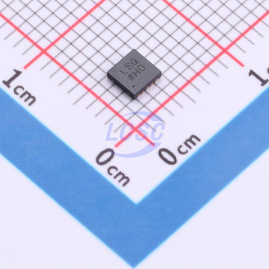
Key Specs Summary(12)
- features
- Over Current Protection;Thermal shutdown;Enable control;Input under-voltage protection
- Number Of Outputs
- 1
- Operating Temperature
- -40℃~+125℃
- Operating Voltage
- 5.5V
- Output Configuration
- Positive
- Output CurrentVerified
- 2A
- Output Type
- Fixed
- Output VoltageVerified
- 3V
- package
- LFCSP-10(3x3)
- Supply Current Iq
- 8mA
- Pin CountEnriched
- 10
- Package Industry NameEnriched
- LFCSP
Datasheet Extracted
Facts extracted directly from the datasheet (sourced)Pin Configuration · 10-Lead LFCSP · 10 pins
| # | Name | Type | Function |
|---|---|---|---|
| 1 | VOUT | output | Regulated Output Voltage. |
| 2 | VOUT | output | Regulated Output Voltage. |
| 3 | VOUT_SENSE | input | Output Sense. VOUT_SENSE is internally connected to VOUT with a 10 Ω resistor. |
| 4 | BYP | passive | Low Noise Bypass Capacitor. |
| 5 | EN | input | Enable. Drive EN high to turn on the regulator; drive EN low to turn off the regulator. |
| 6 | REF_SENSE | input | Reference Sense. Connect REF_SENSE to the REF pin. |
| 7 | REF | output | Low Noise Reference Voltage Output. |
| 8 | VREG | output | Regulated Input Supply Voltage to Low Dropout (LDO) Amplifier. |
| 9 | VIN | power in | Regulator Input Supply Voltage. |
| 10 | VIN | power in | Regulator Input Supply Voltage. |
Absolute Maximum Ratings
| VIN to Ground | -0.3 to +7V | |
| Storage Temperature Range | -65 to +150°C |
Recommended Operating
| Input voltage range | 2.3 to 5.5V | |
| Quiescent current | 4.0mA | IGND at no load |
| Operational Junction Temperature Range | -40 to +125°C |
Thermal
- theta ja
- 53.8
- theta jc
- 15.6
Ordering
- R7
- Tape and Reel
Similar Parts
Reference Designs Using This Part
0 designsManufacturer-validated system circuits with BOM and Gerber files — one step closer to a finished product than the typical circuit in a datasheet.