No Domestic Stock
Request a quote for this part and sellers will provide prices.
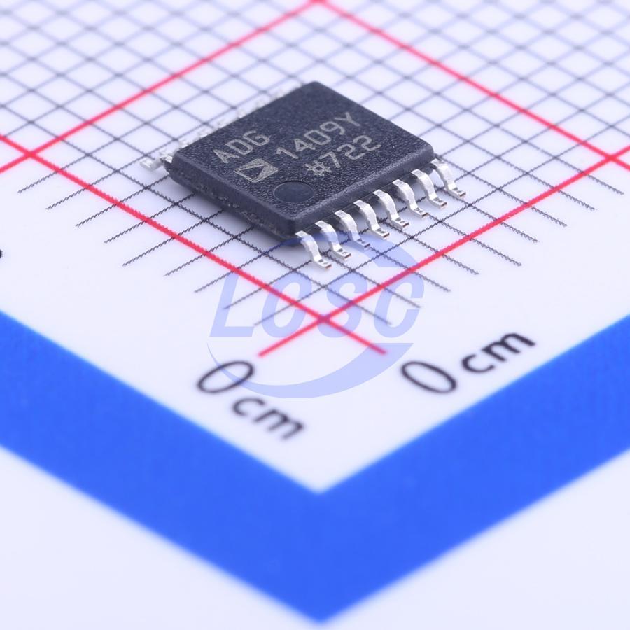
Key Specs Summary(9)
- con
- 90pF
- Number Of Channels
- 4
- ron
- 4Ω
- Operating Temperature
- -40℃~+125℃
- Operating Temperature MaxEnriched
- 125°C
- Operating Temperature MinEnriched
- -40°C
- package
- TSSOP-16
- Pin CountEnriched
- 16
- Voltage Supply
- -15V~15V;12V;-5V~5V
Datasheet Extracted
Facts extracted directly from the datasheet (sourced)Pin Configuration · 16-lead TSSOP · 16 pins
| # | Name | Type | Function |
|---|---|---|---|
| 1 | A0 | input | Logic Control Input |
| 2 | EN | input | Active High Digital Input |
| 3 | VSS | power in | Most Negative Power Supply Potential |
| 4 | S1A | bidirectional | Source Terminal 1A |
| 5 | S2A | bidirectional | Source Terminal 2A |
| 6 | S3A | bidirectional | Source Terminal 3A |
| 7 | S4A | bidirectional | Source Terminal 4A |
| 8 | DA | bidirectional | Drain Terminal A |
| 9 | DB | bidirectional | Drain Terminal B |
| 10 | S4B | bidirectional | Source Terminal 4B |
| 11 | S3B | bidirectional | Source Terminal 3B |
| 12 | S2B | bidirectional | Source Terminal 2B |
| 13 | S1B | bidirectional | Source Terminal 1B |
| 14 | VDD | power in | Most Positive Power Supply Potential |
| 15 | GND | power in | Ground (0 V) Reference |
| 16 | A1 | input | Logic Control Input |
Absolute Maximum Ratings
| VDD to VSS | 35V | |
| VDD to GND | -0.3 to 25V | |
| VSS to GND | +0.3 to -25V | |
| Analog Inputs | VSS - 0.3 to VDD + 0.3 or 30 mAV/mA | whichever occurs first |
| Digital Inputs | GND - 0.3 to VDD + 0.3 or 30 mAV/mA | whichever occurs first |
| Peak Current, S or D | 350mA | Pulsed at 1 ms, 10% Duty Cycle Maximum |
| Storage Temperature Range | -65 to 150°C | |
| Junction Temperature | 150°C |
Recommended Operating
| Operating Temperature Range | -40 to 125°C | Industrial (Y Version) |
Thermal
- unit
- °C/W
- theta ja
- 150.4
- theta jc
- 50
Ordering
- REEL7
- 16-Lead Thin Shrink Small Outline Package [TSSOP] RU-16
Similar Parts
Reference Designs Using This Part
0 designsManufacturer-validated system circuits with BOM and Gerber files — one step closer to a finished product than the typical circuit in a datasheet.