No Domestic Stock
Request a quote for this part and sellers will provide prices.
Key Specs Summary(13)
- Integral Non Linearity
- 1LSB
- interface
- SPI
- Max Supply VoltageEnriched
- 6V
- Min Supply VoltageEnriched
- 2.3V
- Operating Supply VoltageEnriched
- 5.5V
- Operating Temperature
- -40℃~+125℃
- Operating Temperature MaxEnriched
- 125°C
- Operating Temperature MinEnriched
- -40°C
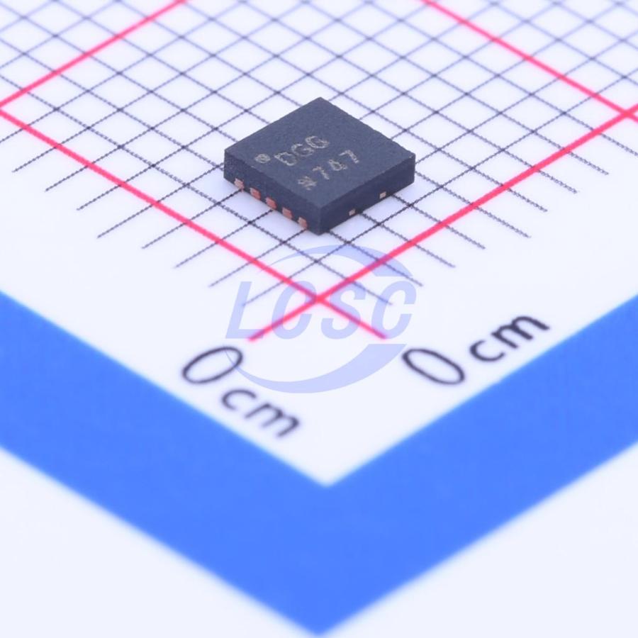
- package
- LFCSP-10(3x3)
- Pin CountEnriched
- 10
- Resolution Bits
- 10
- The Main Fclk
- 5MHz
- Voltage Supply
- 2.3 to 5.5V
Datasheet Extracted
Facts extracted directly from the datasheet (sourced)Pin Configuration · 10-lead LFCSP_WD · 10 pins
| # | Name | Type | Function |
|---|---|---|---|
| 1 | COMP | output | DAC Bias Pin |
| 2 | VDD | power in | Positive Power Supply for the Analog and Digital Interface Sections |
| 3 | CAP/2.5V | power out | 2.5 V regulator output |
| 4 | DGND | power in | Digital Ground |
| 5 | MCLK | input | Digital Clock Input |
| 6 | SDATA | input | Serial Data Input |
| 7 | SCLK | input | Serial Clock Input |
| 8 | FSYNC | input | Active Low Control Input |
| 9 | AGND | power in | Analog Ground |
| 10 | VOUT | output | Voltage Output |
Absolute Maximum Ratings
| VDD to AGND | 6V | |
| VDD to DGND | 6V | |
| AGND to DGND | 0.3V | |
| CAP/2.5V | 2.75V | |
| Digital I/O Voltage to DGND | VDD + 0.3V | |
| Analog I/O Voltage to AGND | VDD + 0.3V | |
| Storage Temperature Range | 150°C | |
| Maximum Junction Temperature | 150°C |
Recommended Operating
| Operating Temperature Range | 125°C | Industrial (B Version) |
Thermal
- theta ja
- 206
- theta jc
- 44