No Domestic Stock
Request a quote for this part and sellers will provide prices.
Key Specs Summary(22)
- Common Mode Rejection Ratio CmrrEnriched
- 70dB
- Gain Bandwidth ProductVerified
- 200MHz
- Ib Input Bias Current
- 500nA
- Input Offset Current Drift Ios Tc
- 0.2nA/℃
- Input Offset Voltage Drift Vos Tc
- 2uV/℃
- Vos Input Offset Voltage
- 200uV
- Maximum Power Supply Range Vdd Vss
- 25.2V
- Number Of Channels
- 1
- Operating Temperature
- -40℃~+125℃
- Output Current
- 35mA
- Output Type
- Single-Ended
- Quiescent Current
- 10.6mA
- Rail To Rail
- Rail-to-Rail Output
- Settling Time
- 20ns
- Single Supply
- 4.5 to 12.6V
- Slew RateVerified
- 1070V/us
- Dual Supply
- -12.6 to 12.6V
- Input Offset Current Ios
- 0.4uA
- Noise Density E N
- 4.5nV/√Hz
- Operating Temperature MaxEnriched
- 85°C
- Operating Temperature MinEnriched
- -40°C
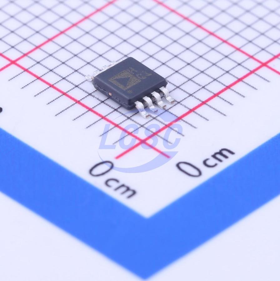
- package
- MSOP-8
Datasheet Extracted
Facts extracted directly from the datasheet (sourced)Pin Configuration · 8-Lead MSOP · 8 pins
| # | Name | Type | Function |
|---|---|---|---|
| 1 | +IN | input | None |
| 2 | -IN | input | None |
| 3 | -VS | power in | None |
| 4 | +VS | power in | None |
| 5 | PD | input | None |
| 6 | OUT | output | None |
| 7 | REF | passive | None |
| 8 | FB | input | None |
Absolute Maximum Ratings
| Supply Voltage | 26.4V | |
| Input Voltage (Any Input) | -VS - 0.3 to +VS + 0.3V | |
| Differential Input Voltage (AD8129) | ±0.5V | VS ≥ ±11.5 V |
| Differential Input Voltage (AD8129) | ±6.2V | VS < ±11.5 V |
| Storage Temperature Range | -65 to +150°C | |
| Junction Temperature | 150°C |
Recommended Operating
| Power Supply Range | 4.5 to 12.6V | single or dual |
Thermal
- theta ja
- 142
Ordering
- Z
- Pb-free part
- #
- lead-free, may be top or bottom marked
Similar Parts
Reference Designs Using This Part
0 designsManufacturer-validated system circuits with BOM and Gerber files — one step closer to a finished product than the typical circuit in a datasheet.