국내 재고 없음
이 부품에 대한 견적을 요청하시면 판매자들이 가격을 제시합니다.
주요 스펙 요약(12)
- features
- Over Current Protection;Thermal shutdown;Enable control;Input under-voltage protection
- Number Of Outputs
- 1
- Operating Temperature
- -40℃~+125℃
- Operating Voltage
- 5.5V
- Output Configuration
- Positive
- Output Current검증
- 600mA
- Output Type
- Fixed
- Output Voltage검증
- 1.8V
- package
- SOIC-8-EP
- Supply Current Iq
- -
- Pin Count보강
- 8
- Package Industry Name보강
- SOIC
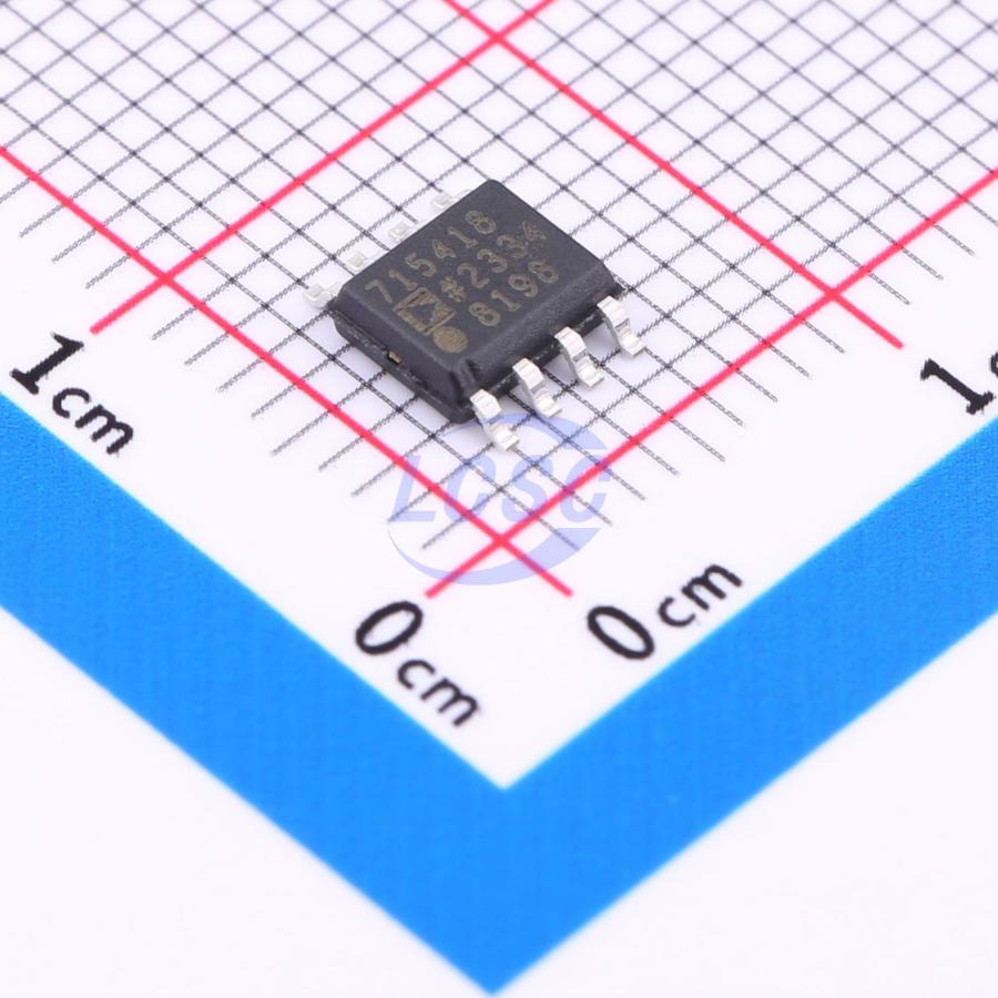
데이터시트 추출 정보
데이터시트에서 직접 추출한 사실 (출처 명시)핀 배치 · 8-Lead SOIC_N_EP · 8 핀
| # | Name | Type | Function |
|---|---|---|---|
| 1 | VREG | power out | Regulated Input Supply Voltage to LDO Amplifier. Bypass VREG to GND with a 10 µF or greater capacitor. |
| 2 | VOUT | power out | Regulated Output Voltage. Bypass VOUT to GND with a 10 µF or greater capacitor. |
| 3 | BYP | passive | Low Noise Bypass Capacitor. Connect a 1 µF capacitor from the BYP pin to GND to reduce noise. Do not connect a load to g |
| 4 | GND | power in | Ground Connection. |
| 5 | REF_SENSE | input | Reference Sense. Connect Pin 5 to the REF pin. Do not connect Pin 5 to VOUT or GND. |
| 6 | REF | power out | Low Noise Reference Voltage Output. Bypass REF to GND with a 1 µF capacitor. Short REF_SENSE to REF for fixed output vol |
| 7 | EN | input | Enable. Drive EN high to turn on the regulator; drive EN low to turn off the regulator. For automatic startup, connect E |
| 8 | VIN | power in | Regulator Input Supply Voltage. Bypass VIN to GND with a 10 µF or greater capacitor. |
절대 최대 정격
| VIN to GND | -0.3 to +7V | |
| Storage Temperature Range | -65 to +150°C | |
| Junction Temperature | 150°C |
권장 동작 조건
| Input voltage range | 2.3 to 5.5V | |
| Quiescent current, IGND | 4mA | no load |
열 특성
- theta ja
- 36.9
- theta jc
- 27.1
오더링 코드
- R7
- 7-inch reel
유사 부품
이 부품을 사용한 Reference Design
0건제조사가 검증한 시스템 회로 + BOM + Gerber 자료. 데이터시트의 typical circuit 보다 한 단계 완제품에 가까움.