주요 스펙 요약(18)
- Common Mode Rejection Ratio Cmrr보강
- 90dB
- Gain Bandwidth Product검증
- 3.5MHz
- Ib Input Bias Current
- 20pA
- Input Bias Current보강
- 20pA
- Input Offset Voltage Drift Vos Tc
- 15uV/℃
- Vos Input Offset Voltage보강
- 3.5mV
- Number Of Channels검증
- -
- Number Of Circuits보강
- 4
- Operating Temperature
- -
- Operating Temperature Max보강
- 85°C
- Operating Temperature Min보강
- -40°C
- Output Current검증
- -
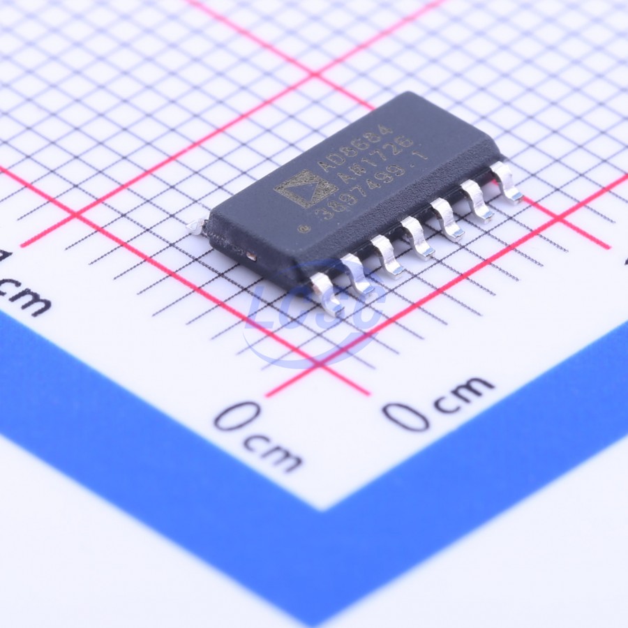
- package
- SOIC-14
- Quiescent Current
- 210uA
- Rail To Rail
- -
- Slew Rate검증
- 9V/us
- Max Supply Voltage보강
- 18V
- Voltage Gain보강
- 20V/mV
데이터시트 추출 정보
데이터시트에서 직접 추출한 사실 (출처 명시)핀 배치 · 14-Lead SOIC_N and 14-Lead TSSOP · 14 핀
| # | Name | Type | Function |
|---|---|---|---|
| 1 | OUT A | output | None |
| 2 | –IN A | input | None |
| 3 | +IN A | input | None |
| 4 | V+ | power in | None |
| 5 | +IN B | input | None |
| 6 | –IN B | input | None |
| 7 | OUT B | output | None |
| 8 | OUT C | output | None |
| 9 | –IN C | input | None |
| 10 | +IN C | input | None |
| 11 | +IN B | input | None |
| 12 | V– | power in | None |
| 13 | –IN D | input | None |
| 14 | OUT D | output | None |
절대 최대 정격
| Supply Voltage | 18V | ± |
| Input Voltage | 18V | ± |
| Differential Input Voltage | 36V | |
| Output Short-Circuit Duration | Indefinite | |
| Storage Temperature Range | -65 to +150°C | |
| Operating Temperature Range | -40 to +85°C | |
| Junction Temperature Range | -65 to +150°C | |
| Lead Temperature (Soldering, 60 sec) | 300°C |
권장 동작 조건
| Supply Voltage Range | 4.5V | ± |
| Supply Voltage Range | 18V | ± |
열 특성
- theta ja
- 120-210
- theta jc
- 35-45
유사 부품
이 부품을 사용한 Reference Design
0건제조사가 검증한 시스템 회로 + BOM + Gerber 자료. 데이터시트의 typical circuit 보다 한 단계 완제품에 가까움.